Q.
The waveforms A and B given below axe given as input to a NAND gate. Then its logic output Y is Voltage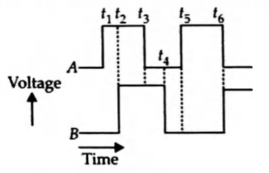
Solution:
Time
$A$
$B$
$Y =\overline{ AB }$
$t _{1}$
1
0
1
$t _{2}$
1
1
0
$t _{3}$
1
1
0
$t _{4}$
0
1
1
$t_5$
0
0
1
$t_6$
1
1
0
NAND gate is the combination of AND and NOT gate and the output of the two inputs ($A$ and $B$)
NAND gate is $Y =\overline{ AB }$
Here, the truth table for the NAND gate will be the following table,
(note 1 for high signal and o for low signal)
| Time | $A$ | $B$ | $Y =\overline{ AB }$ |
|---|---|---|---|
| $t _{1}$ | 1 | 0 | 1 |
| $t _{2}$ | 1 | 1 | 0 |
| $t _{3}$ | 1 | 1 | 0 |
| $t _{4}$ | 0 | 1 | 1 |
| $t_5$ | 0 | 0 | 1 |
| $t_6$ | 1 | 1 | 0 |