Thank you for reporting, we will resolve it shortly
Q.
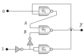
In the circuit shown in the following figure, the value of $Y$ is
NTA AbhyasNTA Abhyas 2020Semiconductor Electronics: Materials Devices and Simple Circuits
Solution:
Lower NOT gate inverts input to zero. NOT gate from NAND gate inverts this output to $1$ and upper NAND gate converts this input $1$ and input $0$ to $1$ .
Thus $A=1$ and $B=1$ become inputs of NAND gate giving final output as zero. Choice A is correct.